WHAT IT IS
Elbrus (Эльбрус) is not one chip. It is a Soviet-then-Russian computing brand that has covered three different instruction sets: the Burtsev large systems of the 1970s–80s, a SPARC-compatible line called Elbrus-90micro, and the modern MCST VLIW microprocessors (architecture E2K). The name is the mountain. The silicon under it changed twice.
Design lineage: Lebedev Institute of Precision Mechanics and Computer Engineering (ITMVT), then INEUM, then MCST (Moscow Center of SPARC Technologies — the name is historical; the current flagship ISA is not SPARC). The machines that filled a floor of Don-2N and Noginsk-9 were Elbrus-1 and Elbrus-2. The chips sold in 2026 as Elbrus-2S3 and Elbrus-16S are E2K generation 6.
WHY BUILD IT AT HOME
Strategic computers in air defence, nuclear design, spaceflight control and later C2 were not to depend on a foreign instruction set or a foreign fab’s willingness to ship. Tagged memory and later VLIW were also argued as a security feature: binary compatibility with x86 is an optional translation layer, not the native machine, so a Western implant written to Intel microcode assumptions does not drop in. After 2014 and especially after 2022, the argument became blunt — TSMC stopped, import substitution became policy, and a domestic ISA was the only way to keep compiling classified code when Xeon boards disappeared.
That does not make Elbrus faster than a contemporary Epyc. It makes the instruction stream and, when the mask works, the supply chain, a Russian document. Fabrication of the 16 nm parts was still offshore until sanctions; mid-2026 reporting described resumed lots of 2S3 and 16S from a “friendly-country” line after a four-year gap. Design sovereignty and fab sovereignty are not the same sentence. The one E2K CPU that was actually cut on a Russian line in volume is Elbrus-2SM at Mikron, Zelenograd.
GENERATION I — ELBRUS-1 AND ELBRUS-2
Vsevolod Burtsev’s machines, influenced by Burroughs large systems: tagged architecture, stack-oriented execution, ALGOL-68 as a system language. Elbrus-1 (late 1970s) used TTL, under 15 million operations per second. Elbrus-2 (design from 1978, prototypes 1984, series from about 1985–87) switched to ECL, about 20 MHz, ten processors (eight live plus two spare in common descriptions), on the order of 125 million ops/s for the box and 12.5 million per processor on a Gibson mix. Memory up to 144 MB. Water-cooled. About 200 processor sets built through 1992.
Where they sat: Don-2N (four ten-processor Elbrus-2 complexes in open accounts), the A-135 command-computing post at Sofrino, Noginsk-9 / TsKKP (Elbrus-1 from 1984, Elbrus-2 from 1995), Mission Control, Arzamas-16 and Chelyabinsk-70. This is the “brain of Moscow ABM” machine in the older articles of this database. The 2021 Don-2N modernization replaced that floor with Elbrus-90S at about 100 billion ops/s.
SIDE LINE — ELBRUS-90MICRO (SPARC)
1998–2010 computers on MCST SPARC CPUs: R80, R150, R500, R500S, MCST-4R, clocks from 80 MHz to 1 GHz. Same brand, different ISA. Open notes put Elbrus-90micro in S-400 control chains. MSVS (MCBC) listed SPARC / Elbrus-90micro as a supported platform. Do not confuse this SPARC board with an E2K-16S.
GENERATION II — VLIW, BABAYAN, E2K
After Burtsev, Boris Babayan’s team built Elbrus-3 (1990), a 16-processor VLIW machine and one of the early wide-word systems. That architecture, not the Burtsev stack, became Elbrus-2000 (E2K) in 2001 and then the MCST microprocessor line.
VLIW / EPIC means the compiler, not an out-of-order engine on the die, packs independent operations into one long instruction word. An E2K core exposes on the order of six ALU channels; later generations quote up to 23–50 operations per clock depending on how vector and FMA slots are counted. x86 spends silicon on speculation, register renaming and a huge scheduler. Elbrus spends silicon on execution units and asks the compiler to keep them fed. When the compiler is good and the code is dense math, the peak flop rating looks competitive per watt. When the code is branchy desktop software, the same chip looks slow next to a Ryzen that guesses ahead in hardware. Binary translation of x86 exists on later E2K generations, including hardware-assist for virtualization on v6; it is a compatibility layer, not the native speed path.
Register file in MCST literature: 256 × 84-bit. Explicit parallelism is the selling point for DSP, crypto and linear algebra — the jobs Don-2N and SKKP actually run.
MICROPROCESSOR LADDER
Elbrus-2000 / 3M1 — 2005, 130 nm, 300 MHz, 1 core, ~2.4/4.8 GFLOPS (64/32-bit). Elbrus-S — 2010, 90 nm, 500 MHz, 1 core. Elbrus-2S+ — 2011, dual core + DSP blocks, 500 MHz, TSMC 90 nm. Elbrus-2SM — 2014, Mikron 90 nm, 300 MHz, dual core, no DSP. Domestic cut. See below. Elbrus-4S — 2014, 65 nm, 800 MHz, 4 cores, ~25/50 GFLOPS, 45 W. Elbrus-1S+ — 2016, 40 nm SoC with GPU, ~1 GHz, embedded. Elbrus-8S — 2015–16, 28 nm, 1.3 GHz, 8 cores, ~125/250 GFLOPS, 80 W. Elbrus-8SV — serial from ~2020, 28 nm, 1.5 GHz, 8 cores, ~288/576 GFLOPS, DDR4, 90 W. Elbrus-2S3 — gen 6, 16 nm, 2 GHz, 2 CPU cores plus GPU/video blocks, ~10–15 W, DDR4-3200, laptops and embed. Resurfaced on the market 2024–26. Elbrus-12S — gen 6, 16 nm, 12 cores, 2 GHz, ~95 W (planned/limited). Elbrus-16S (1891VM038) — gen 6, 16 nm TSMC-class, 16 cores, 2.0 GHz (1.8 GHz B-bin), L2 1 MB/core, L3 32 MB, 8-channel DDR4-3200 ECC, up to 4 sockets via IPCC links at 16 GB/s each, PCIe 3.0, ~750 GFLOPS FP64 / 1.5 TFLOPS FP32, 130 W. Server flagship. Elbrus-32C — gen 7, planned ~7 nm class, 32 cores, 2.5 GHz, DDR5, PCIe 5.0, engineering sample talk for 2025; peak brochure figures 1.5 TFLOPS FP64 / 3 TFLOPS FP32 in one table, higher in others that assume vector/ML modes. Treat 32C as the announced next die, not a volume part in 2026.
DOMESTIC FAB — MIKRON AND ELBRUS-2SM
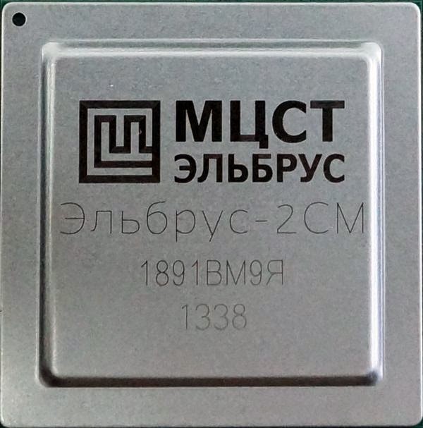
Most of the fast E2K parts were drawn in Moscow and cut at TSMC. The exception that matters for sovereignty talk is Elbrus-2SM (Эльбрус-2СМ, 1891ВМ9Я, working name Elbrus-1C during the OKR). It is a 2S+ stripped of the four Elcore-09 DSP cores and redrawn onto Mikron’s 90 nm standard-cell libraries so the mask could run in Zelenograd.
AO Mikron (NIIME i Mikron), Zelenograd, dates to 1964 and was one of the three Soviet IC houses with Angstrem and Integral. FAB-150 still does power and bipolar parts at micron scales. FAB-200 is the CMOS line cited at 250–65 nm with 6–8 metal layers. 90 nm was brought up in 2012 with Rosnano money. In December 2014 Mikron and MCST announced pilot production of 2SM and the compact Monokub-M board. First time a Russian fab had cut a general-purpose CPU with more than 300 million transistors.
Elbrus-2SM published card (MCST): Architecture: E2K VLIW, two universal cores, up to 23 ops/clock per core. Clock: 300 MHz (2S+ on TSMC ran 500 MHz; the domestic process and the LP low-leakage variant cost frequency). Peak: more than 12 billion operations per second; 4.8 GFLOPS FP64 / 9.6 GFLOPS FP32 in the comparison tables against 2S+. L1: 64 KB data + 64 KB instruction per core. L2: 2 MB shared (some OKR sheets said 1 MB per core; MCST production sheet lists 2 MB total). Memory: two channels DDR2-533 ECC, 8.5 GB/s aggregate. Coherent multiprocessor: up to four CPUs, three inter-CPU links at 4 GB/s each. I/O / RemoteDMA: two channels at 2 GB/s; south bridge KPI. Package: HFCBGA 1296. Power: ~20 W. Rails 1.2 / 1.8 / 2.5 V. Temperature: −40 to +85 °C. Transistors: about 300 million (2S+ was 368 million with the DSP complex). Production start: 2014.
Monokub-M was the first board: mini layout, PCIe 1.0, Gigabit Ethernet, USB 2.0, VGA/DVI, SATA 2.0, CompactFlash, RS-232, GPIO. That is thin-client, cash-register, and hardened-embed territory — exactly the market later commentators assigned to a 90 nm domestic part.
Mikron cannot cut 16S. After 2022, when TSMC dropped the 28 nm and 16 nm lots, MCST talked about moving more masks to Zelenograd. Open industry comment was blunt: 90 nm is a generation walk-back; 28 nm in Russia was not a near-term promise. 2SM remains the proof that an E2K die can leave a Russian clean room. 16S and 2S3 remain the proof that the fast dies still need someone else’s lithography. The 2026 restart of those faster parts was described as contract production in a friendly state, not as FAB-200 suddenly doing 16 nm.
Angstrem is the other Zelenograd name in the same story. Neither plant is TSMC. Domestic Elbrus silicon, as of the public record, is 2SM-class 90 nm and whatever older analog/digital support chips Mikron already sold. Everything quicker was imported wafers with a Russian netlist.
HOW A MODULE IS WIRED
A modern server module is not a single chip talking to a Southbridge across a 1990s bus. Elbrus-16S brings the third-generation peripheral controller on die. Two or four CPUs share memory over IPCC interconnects (three 16 GB/s links in the four-socket drawing; one link multiplexed with PCIe). That is ccNUMA in the same family as Elbrus-MV3S1/C (2009) and as the four-socket 2SM drawing at 4 GB/s links. Cooling and board design follow the TDP: 20 W for 2SM, 10 W for 2S3, 130 W for 16S. Software sees Linux (including Elbrus Linux / OS Elbrus) or, on older military boxes, MSVS on the SPARC cousins.
WHERE IT IS USED
Elbrus-1/2: A-135 / Don-2N, SKKP catalogue shop, TsUP, weapons labs. Elbrus-90micro: S-400-class control and other SPARC-era military computers. E2K: government and defence servers and workstations that must stay off Xeon; industrial and scientific boxes in the import-substitution catalogue; 2S3 in rugged laptops and embed; 2SM in compact domestic-fab machines where a foreign wafer is not acceptable. Peak flop claims are aimed at the same numerical jobs the 1980s machines did — trajectories, crypto, signal processing — not at running a Western game engine.
COMPARED WITH X86 AND ARM
x86/ARM: hardware schedules a conventional ISA; huge installed software; fabs at 5–3 nm in the West and East Asia. E2K: compiler schedules a wide word; modest software ecosystem; binary translation for x86 when needed; 16 nm parts in the current volume story, 90 nm when the wafer must be Russian; security argument is “we own the ISA and the compiler.” Baikal is the other Russian server brand and is ARM, not VLIW. Choosing Elbrus is choosing an original architecture and a small tool chain. Choosing Baikal is choosing a licensed ARM core and a larger Linux world. Policy has funded both.
FUTURE
Gen 7 (32C) is the published next step: more cores, DDR5, on-die ML/FP16 talk. Whether it reaches series depends on a fab that will take the mask. 2026 production news is the restart of 2S3 (thousands) and 16S (tens in early lots, per trade press) after the 2022 TSMC cut. OpenElbrus and Linux ports are the attempt to grow the userland so the chip is not only a closed military compile target. The constraint is not the mountain’s name. It is process node, yield, and compilers — and the gap between Mikron’s 90 nm and the 16 nm the flagship needs.
IN ONE SENTENCE
Elbrus is a fifty-year Russian computing brand that began as Burtsev’s tagged ECL mainframes in Don-2N, passed through a SPARC side line in the S-400 era, and is now MCST’s E2K VLIW microprocessors — 2SM the 90 nm part Mikron actually cut in Zelenograd, 2S3 and 16S the 16 nm parts that still need a foreign fab, 32C on the roadmap — built so classified arithmetic does not have to run on someone else’s ISA.